
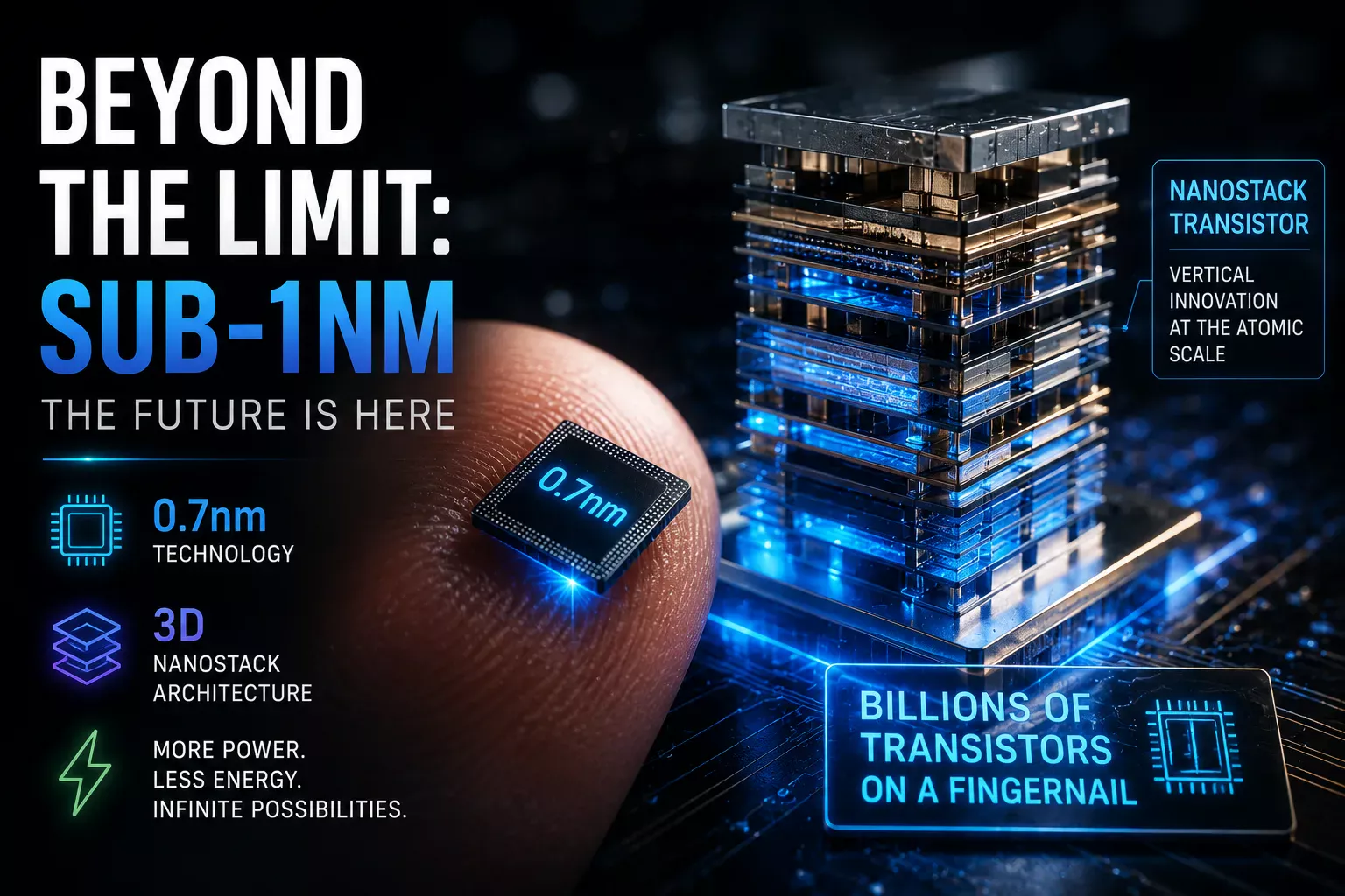
In the relentless pursuit of more powerful and efficient computing, the semiconductor industry has consistently pushed the boundaries of physics, shrinking components to scales once thought impossible. This ongoing miniaturization has been the bedrock of technological progress, enabling everything from the smartphones in our pockets to the vast cloud data centers that power our digital lives. A significant moment in this journey occurred with the announcement from IBM, revealing the development of the world’s first sub-1 nanometer (nm) semiconductor technology. This achievement, built upon a novel 3D “nanostack” transistor architecture at the 0.7 nm (7 angstrom) node, represents a substantial stride forward in chip design and manufacturing.
This breakthrough is not merely an incremental improvement; it signifies a fundamental rethinking of how transistors are built and arranged. For decades, the industry has followed Moore’s Law, doubling the number of transistors on a chip roughly every two years. As physical limits are approached, maintaining this pace requires increasingly ingenious engineering. IBM’s latest innovation addresses these challenges directly, laying a foundation for the next generation of computing capabilities that will impact artificial intelligence (AI), cloud infrastructure, and countless other applications.
Beyond the Horizon: The 0.7 Nanometer Threshold
For years, the semiconductor industry has measured progress in nanometers, a unit of length equivalent to one-billionth of a meter. Each reduction in this metric typically means more transistors can be packed onto a silicon die, leading to increased performance and energy efficiency. While 2 nm chips were already pushing the limits of current manufacturing techniques, IBM’s move to 0.7 nm represents a leap into a territory previously only theoretical.
The scale of this advancement is difficult to grasp without context. A human hair is approximately 75,000 nanometers thick. The 0.7 nm node is roughly 100,000 times smaller than a human hair, placing it at the atomic scale where quantum effects become increasingly prominent. Successfully designing and fabricating functional transistors at this dimension requires mastery over materials science, lithography, and intricate engineering processes.
This achievement is a testament to the persistent research and development efforts within the semiconductor sector, particularly from entities like IBM, which has a long history of foundational contributions to chip technology. The sheer precision required to etch circuits and place components at this scale demands advanced techniques, pushing the capabilities of extreme ultraviolet (EUV) lithography and other cutting-edge fabrication methods to their absolute limits.
A New Dimension in Transistor Design: The Nanostack Architecture
The ability to shrink features to 0.7 nm is impressive, but the real innovation lies in how these tiny transistors are constructed. IBM’s solution is a revolutionary 3D “nanostack” transistor architecture. Traditional planar transistors arrange components side-by-side on a two-dimensional surface. As these components shrink, the challenges of leakage current and control become more pronounced. FinFET (Fin Field-Effect Transistor) designs introduced a 3D gate structure, offering better control, but even FinFETs face scaling limitations.
The nanostack architecture takes this three-dimensional approach further. Instead of simply wrapping the gate around a fin, nanostack designs allow for the stacking of multiple gate-all-around (GAA) nanosheets or nanowires vertically. This vertical arrangement offers significant advantages in terms of density and electrical control. By stacking transistors, engineers can achieve higher transistor counts within the same footprint, effectively using the third dimension to bypass some of the physical constraints of a purely 2D layout.
This architectural shift is critical for continued scaling. It moves beyond the limitations of traditional scaling by introducing a new paradigm for how transistors interact and are integrated onto the silicon wafer. The nanostack approach provides better electrostatic control over the channel, which translates directly into improved performance and reduced power consumption, even at these minuscule dimensions. This method of construction is not just about making things smaller; it’s about making them smarter and more efficient.
graph TD
    A[Input/Output Layer] --> B{Interconnects}
    B --> C[Power Delivery Layer]
    C --> D[Stacked Transistor Layers]
    D --> E[Gate-All-Around (GAA) Nanosheets]
    E --> F[Channel Material]
    F --> G[Substrate]

    subgraph 3D Nanostack Transistor
        direction TB
        D -- Vertical Integration --> E
        E -- Multiple Layers --> F
    end

    style A fill:#f9f,stroke:#333,stroke-width:2px
    style B fill:#bbf,stroke:#333,stroke-width:2px
    style C fill:#fbb,stroke:#333,stroke-width:2px
    style D fill:#afa,stroke:#333,stroke-width:2px
    style E fill:#faa,stroke:#333,stroke-width:2px
    style F fill:#ddf,stroke:#333,stroke-width:2px
    style G fill:#ccf,stroke:#333,stroke-width:2px
Above: A simplified representation of the 3D nanostack transistor architecture, illustrating the vertical integration of components to achieve higher density and improved electrical characteristics.
Unprecedented Density: Billions on a Fingernail
The immediate and most striking consequence of the 0.7 nm node and nanostack architecture is the staggering increase in transistor density. IBM’s breakthrough chip manages to pack nearly 100 billion transistors onto a die approximately the size of a fingernail. To put this into perspective, this almost doubles the transistor density achieved by IBM’s 2 nm chip, which was introduced just in 2021. This rapid progression highlights the exponential nature of semiconductor advancement when fundamental architectural innovations are introduced.
Such immense density means that future processors can handle significantly more complex computations simultaneously. Each transistor acts as a tiny switch, and with 100 billion switches available, the potential for parallel processing and intricate logical operations expands dramatically. This is not just a numbers game; it directly translates to the ability to execute more instructions per clock cycle, manage larger datasets, and run more sophisticated algorithms. This level of integration is essential for addressing the growing computational demands across various sectors.
The implications for system designers are profound. With more transistors in a given area, the physical footprint of high-performance computing components can shrink, leading to more compact devices and more powerful servers in existing data center racks. This density also offers flexibility, allowing chip designers to either integrate more functional units (like CPU cores, AI accelerators, or specialized processing units) or to allocate more resources to on-chip memory and cache, further boosting performance.
Performance and Efficiency: Fueling the AI and Cloud Epoch
The gains from the 0.7 nm technology extend beyond mere transistor count; they translate into substantial improvements in both performance and energy efficiency. The sub-1 nm technology is projected to deliver up to 50% more performance compared to IBM’s 2 nm chips. Alternatively, it can offer up to 70% greater energy efficiency at the same performance level. This dual benefit — higher performance or lower power consumption — provides critical flexibility for different application requirements.
For sectors like generative AI, these improvements are transformative. Training large language models (LLMs) and complex neural networks requires immense computational power and significant energy. Chips with 50% more performance can drastically reduce training times, allowing researchers and developers to iterate faster and build more sophisticated AI models. The ability to run AI workloads with 70% greater energy efficiency is equally vital, helping to mitigate the rapidly growing carbon footprint of AI data centers. Explore how AI is reshaping concrete’s future.
Cloud infrastructure, the backbone of modern digital services, stands to benefit immensely. Cloud providers are constantly seeking ways to improve the performance-per-watt of their servers to reduce operational costs and environmental impact. Chips offering significantly better energy efficiency mean that data centers can achieve higher computational throughput without increasing power consumption, or even reduce power consumption for existing workloads. This directly impacts the scalability and sustainability of cloud services, from streaming platforms to enterprise applications. The constant demand for more processing power in the cloud drives innovations like these. For a deeper look into the future of cloud and edge computing, consider the shift towards localized AI processing.
Memory’s Next Leap: SRAM Scaling Reimagined
Beyond the core logic transistors, the nanostack architecture also brings significant advancements to on-chip memory. Specifically, it enabled a 40% SRAM (Static Random-Access Memory) scaling. SRAM is crucial for processor caches due to its speed, though it consumes more power and occupies more area than other memory types. For over a decade, SRAM scaling has presented a formidable challenge, with improvements becoming increasingly difficult to achieve.
This 40% scaling marks a major step change in memory density that the semiconductor industry has not observed in over ten years. The ability to integrate more SRAM directly onto the chip means larger and faster caches. Larger caches reduce the need for the processor to access slower off-chip main memory, thereby significantly improving overall system performance. This is particularly important for data-intensive applications and AI workloads, where quick access to frequently used data can be a major bottleneck.
Improved SRAM density directly enhances the efficiency of computational tasks by providing data closer to the processing units. This reduces latency and increases throughput, making the entire chip more responsive and powerful. The synergy between advanced logic transistors and scaled SRAM creates a more balanced and potent processing unit, capable of handling the complex demands of future software and AI algorithms. This holistic approach to chip design, addressing both logic and memory, is what truly sets this breakthrough apart.
The Road Ahead: Implications for the Digital Ecosystem
IBM’s 0.7 nm chip technology is currently a research breakthrough, demonstrating what is technically feasible. The journey from research and development to mass production is often long and complex, involving immense capital investment, refinement of manufacturing processes, and collaboration across the global semiconductor supply chain. However, the unveiling of such a technology provides a clear roadmap for the industry, indicating the direction of future silicon innovation.
This development has broad implications for the digital ecosystem. For device manufacturers, it signals the potential for even more powerful and energy-efficient components, enabling new product categories and enhanced capabilities in existing ones. For software developers, it means access to computing resources that can run more sophisticated applications, from advanced simulations to real-time AI inference at the edge. The continuous push for smaller, faster, and more efficient chips underpins virtually every aspect of technological advancement.
The challenge remains to transition this laboratory success into commercial viability at scale. This involves overcoming hurdles related to defect rates, cost-effective manufacturing, and integrating these advanced processes into existing foundry operations. Nevertheless, the announcement from IBM solidifies its position as a leader in semiconductor research and underscores the ongoing innovation required to meet the ever-increasing demands of the digital age. The future of computing, with its immense requirements for AI, data processing, and interconnected systems, will rely heavily on such foundational advancements. For insights into other foundational technologies that could shape our future, one might consider Read more in our article on The Quantum Apocalypse: How Unbreakable Math Will Shield Your Data From Tomorrow’s Supercomputers.
Key Takeaways
- Sub-1 Nanometer Breakthrough: IBM has developed the world’s first 0.7 nm (7 angstrom) semiconductor technology, a significant leap beyond current 2 nm chips.
- 3D Nanostack Architecture: The innovation relies on a revolutionary 3D “nanostack” transistor design, allowing for vertical integration and improved control.
- Unprecedented Transistor Density: The new chip packs nearly 100 billion transistors onto a fingernail-sized die, almost doubling the density of 2 nm chips.
- Performance and Energy Efficiency Gains: Projected to deliver up to 50% more performance or 70% greater energy efficiency compared to 2 nm chips.
- Impact on AI and Cloud: These gains are crucial for supercharging generative AI workloads and enhancing cloud infrastructure capabilities.
- Major SRAM Scaling: The nanostack architecture enabled a 40% SRAM scaling, a critical advancement in memory density not seen in over a decade.
FAQ
Q1: What does “sub-1 nanometer” mean in practical terms?
A: “Sub-1 nanometer” refers to transistor gate lengths or critical dimensions smaller than one nanometer. In this case, IBM achieved 0.7 nanometers (7 angstroms). Practically, it means transistors are incredibly small, allowing billions to fit on a tiny chip, leading to vastly increased processing power and efficiency.
Q2: How does the 3D nanostack transistor architecture differ from previous designs?
A: Traditional transistors are largely planar, or use FinFETs which wrap a gate around a fin-like structure. The 3D nanostack architecture involves vertically stacking multiple gate-all-around (GAA) nanosheets or nanowires. This vertical arrangement allows for greater transistor density within the same footprint and provides superior electrical control, reducing leakage and improving performance.
Q3: What are the primary benefits of this 0.7 nm chip for generative AI?
A: For generative AI, the chip offers two main benefits: up to 50% more performance, which accelerates the training and inference of complex AI models, and up to 70% greater energy efficiency, which helps reduce the substantial power consumption associated with large-scale AI computations in data centers.
Q4: Why is a 40% SRAM scaling significant?
A: SRAM (Static Random-Access Memory) is used for fast on-chip caches. Scaling SRAM has been a major challenge for over a decade. A 40% scaling means significantly more SRAM can be integrated onto the chip. This results in larger and faster caches, reducing the need to access slower external memory, thereby boosting overall processor speed and efficiency, especially for data-intensive applications.
Q5: When can we expect to see this 0.7 nm technology in commercial products?
A: While IBM has demonstrated the technology in a research setting, bringing it to mass commercial production typically takes several years. This involves extensive engineering, manufacturing process refinement, and significant investment. It serves as a foundational step, indicating the future direction for advanced chip manufacturing.
The unveiling of IBM’s 0.7 nm chip technology marks a pivotal moment in the ongoing evolution of computing. It underscores the continuous innovation required to meet the accelerating demands of data-intensive applications, particularly in the burgeoning fields of artificial intelligence and cloud computing. This architectural ingenuity, pushing the boundaries of miniaturization and efficiency, sets a compelling precedent for the next phase of digital transformation, promising a future where computational capabilities are even more profound and pervasive.
